Selection Criteria for Power Management ICs (PMICs)

What is Power IC Working Function complete Detail electronics - Mobile -computer hardware
Through a certain circuit layout, power management turns various power inputs into output voltages that fit the needs of the system. The power supply has a direct impact on system performance, and the power management chip is the fundamental component that influences power supply performance (PMIC). It is vital to comprehend the power management chip's selection criteria (PMIC).
Ⅰ. Understand the power usage environment
To choose the right power management components, you must first comprehend the application's environmental conditions, such as the system's input and output characteristics, and so on. These are some of the factors to consider:
Is it an alternating current (AC) or a direct current (DC) power source?
Is it USB or battery powered while using direct power?
Is the input voltage higher or lower than the output voltage that you want?
What is the load current that is required?
Is the load noise-sensitive, does it require a constant current (like in LED applications), or does it require a variable current?
Is there enough room for installation? More power in a smaller package.
Different applications have unique needs that necessitate specialized power conversion systems and power management ICs. Low-dropout linear regulators (LDOs), DC /DC switching converters, and other ubiquitous ICs are among them. A buck converter (Buck), a boost converter (Boost), and a boost/buck converter are three types of DC/DC switching converters (Buck-boost).
The input-output voltage difference is the first consideration when building a circuit (VIN - VOUT). Second, based on the application's specific needs, such as efficiency, thermal limitations, noise, complexity, and cost, choose the best power management chip (IC).
Ⅱ. There is an option when VOUT is less than VIN
The needed output current and VIN/VOUT ratio are crucial parameters to consider when choosing LDO or Buck when VOUT is smaller than VIN.
(1) Select LDO for low VIN/VOUT applications
The LDO Linear Regulator (Low Dropout Linera Regulator) regulates the output voltage by controlling the conduction of the pass element in a linear fashion. It provides a precise and noise-free output voltage and can respond quickly to load changes at the output end. As a result, it's perfect for low-noise, low-current, and low-VIN/VOUT applications.
Consider the input and output voltage ranges, the LDO's current level, and the package's heat dissipation capability when selecting an LDO. The minimal voltage of VIN - VOUT within the configurable range is referred to as the LDO voltage difference.
In micropower applications, the LDO quiescent current IQ must be low enough to avoid needless battery drain; such applications require specific, low quiescent current IQ low dropout Linear Regulators (LDOs).
However, linear regulation means that the power dissipated by the linear regulator's pass element is equal to the voltage difference between the input and output times the average load current. Excessive extra power losses are caused by both high VIN/VOUT ratios and high load currents. Larger package sizes are required for low dropout linear regulators (LDOs) with increased power consumption, which increases cost, PCB space, and thermal energy consumption.

Figure. 1 LDO Basic Circuit Diagram
When the LDO power dissipation exceeds ~0.8W, it is wiser to switch to a Buck buck converter as an alternative.
(2) Buck converter is selected when VIN/VOUT is high
Buck regulators are switching buck converters that may give high efficiency and flexibility output when the VIN/VOUT ratio and load current are both high. Buck converters (Bucks) are also known as buck regulators (buck regulators) and step-down switching regulators due to their wide range of applications (DC-DC step-down switching regulators). The three terms all refer to the same item.
An internal high-side MOSFET and a low-side MOSFET serve as synchronous rectifiers in most buck converters, and an internal duty-cycle control circuit alternately turns them on and off (ON/OFF) to regulate the average output voltage. An external LC filter can be used to filter the noise created by switching.

Figure. 2 Buck Converter Basic Circuit Diagram
The power consumption is low because the two MOSFETs are switched on and off alternately. The duty cycle can be controlled to provide an output with a higher VIN/VOUT ratio. The internal MOSFET's on-resistance RDS(ON) determines the buck converter's current handling capability, while the MOSFET's voltage rating determines the maximum input voltage. The amount of the ripple voltage at the output is determined by the switching frequency and the external LC filter components; the filter components used in a buck converter with a higher switching frequency can be smaller, but the power consumption caused by switching will increase.
At light loads, a buck converter with pulse skip mode (PSM) reduces its switching frequency, hence enhancing efficiency. For applications that require a low-power standby state, this capability is critical.
Some particular buck topologies, such as ACOT, offer a very quick loop response and are ideal for power applications requiring a very fast load transient response, such as DDR, Core SoC, FPGA, and SIC.
Ⅲ. Select boost converter when VOUT is higher than VIN
In cases where VOUT is greater than VIN, boost regulators are utilized to boost the input voltage to a higher output value. The inductor is charged through the internal MOSFET, and when the MOSFET is turned off, the inductor is discharged to the load through the rectifier. The inductor voltage is reversed when the inductor is charged and discharged, raising the output voltage above VIN.
A boost converter's usual circuit contains an inductor, a power MOSFET, a rectifier diode, a control IC, and input and output capacitors. A typical retrofit setup includes two MOSFETs, one of which substitutes the rectifier diode and switches on when the power switch is turned off.
MOSFETs have a reduced voltage drop, which minimizes power dissipation while improving the regulator's efficiency.
The boost ratio VOUT/VIN is determined by the MOSFET switch's ON/OFF duty cycle, and the duty cycle is also controlled by the feedback loop to maintain a constant output voltage. The output capacitor acts as a buffer, reducing output voltage ripple. The maximum load current is determined by the MOSFET current absolute maximum rating and the boost ratio, whereas the maximum output voltage is determined by the MOSFET voltage absolute maximum rating. To accomplish the effect of synchronous rectification, certain boost converters will merge the rectifier with the MOSFET.

Figure. 3 Boost Converter Basic Circuit Schematic
Ⅳ. Choosing a Buck-Boost Converter When the Input Voltage Is Uncertain
In applications where the input voltage varies, either lower or higher than the output voltage, a boost-buck regulator is utilized. When VIN is more than VOUT, the four internal MOSFET switches automatically set up as a buck converter, and when VIN is less than VOUT, they transition to boost operation. This makes the buck-boost converter suitable for battery -powered applications, particularly when the battery voltage is lower than the regulated output voltage, which helps to increase battery life. Higher efficiency are attained since the four-switch buck-boost converter operates in a fully synchronous mode. Buck mode has a higher output current capability than boost mode because boost mode requires more switching current under the same load conditions.
The maximum input and output voltage range is determined by the MOSFET's voltage absolute maximum ratings. A buck-boost converter with only a single switch and rectifier can be utilized in situations where the output voltage does not need to be referred to ground, such as LED drivers. The output voltage is usually related to VIN.

Figure. 4 Buck-Boost Converter with Four Internal Switches
The four converter topologies described above are used by the majority of power management components. External MOSFET mode can be considered for some particular applications, such as those requiring a very large switching current (e.g. >10A). A specialized power supply monitoring IC can be used to monitor power supply overvoltage or under voltage conditions.
1. What does rsense in power management chips mean? what's the effect?
Current sense resistor, measure the current in the line by measuring the voltage drop across Rsense.
2. What are the commonly used power management chips for motherboards?
The function of the motherboard power management chip is to output the supply or control voltage of each channel after internal adjustment according to the feedback information in the circuit.
3. What is the application range of power management chips?
The power management chip is responsible for the transformation, distribution, detection and other power management of the power in the electronic equipment system. The power management chip is indispensable to the electronic system, and its performance has a direct impact on the performance of the whole machine.
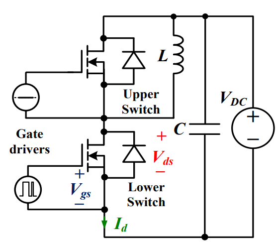
 Discovering New and Advanced Methodology for Determining the Dynamic Characterization of Wide Bandgap DevicesSaumitra Jagdale15 March 20242471
For a long era, silicon has stood out as the primary material for fabricating electronic devices due to its affordability, moderate efficiency, and performance capabilities. Despite its widespread use, silicon faces several limitations that render it unsuitable for applications involving high power and elevated temperatures. As technological advancements continue and the industry demands enhanced efficiency from devices, these limitations become increasingly vivid. In the quest for electronic devices that are more potent, efficient, and compact, wide bandgap materials are emerging as a dominant player. Their superiority over silicon in crucial aspects such as efficiency, higher junction temperatures, power density, thinner drift regions, and faster switching speeds positions them as the preferred materials for the future of power electronics.
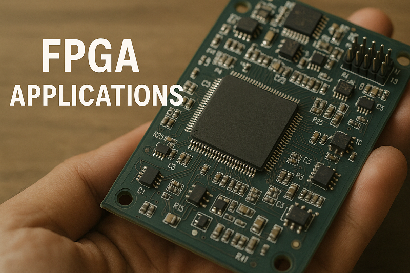
Read More A Comprehensive Guide to FPGA Development BoardsUTMEL11 September 202514694
This comprehensive guide will take you on a journey through the fascinating world of FPGA development boards. We’ll explore what they are, how they differ from microcontrollers, and most importantly, how to choose the perfect board for your needs. Whether you’re a seasoned engineer or a curious hobbyist, prepare to unlock new possibilities in hardware design and accelerate your projects. We’ll cover everything from budget-friendly options to specialized boards for image processing, delve into popular learning paths, and even provide insights into essential software like Vivado. By the end of this article, you’ll have a clear roadmap to navigate the FPGA landscape and make informed decisions for your next groundbreaking endeavor.
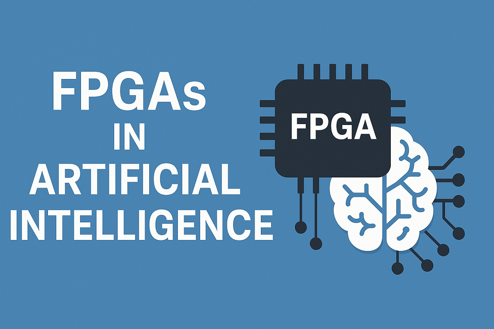
Read More Applications of FPGAs in Artificial Intelligence: A Comprehensive GuideUTMEL29 August 20253608
This comprehensive guide explores FPGAs as powerful AI accelerators that offer distinct advantages over traditional GPUs and CPUs. FPGAs provide reconfigurable hardware that can be customized for specific AI workloads, delivering superior energy efficiency, ultra-low latency, and deterministic performance—particularly valuable for edge AI applications. While GPUs excel at parallel processing for training, FPGAs shine in inference tasks through their adaptability and power optimization. The document covers practical implementation challenges, including development complexity and resource constraints, while highlighting solutions like High-Level Synthesis tools and vendor-specific AI development suites from Intel and AMD/Xilinx. Real-world applications span telecommunications, healthcare, autonomous vehicles, and financial services, demonstrating FPGAs' versatility in mission-critical systems requiring real-time processing and minimal power consumption.
Read More 800G Optical Transceivers: The Guide for AI Data CentersUTMEL24 December 20253838
The complete guide to 800G Optical Transceiver standards (QSFP-DD vs. OSFP). Overcome supply shortages and scale your AI data center with Utmel Electronic.
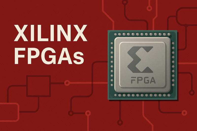
Read More Xilinx FPGAs: From Getting Started to Advanced Application DevelopmentUTMEL09 September 20254299
This guide is your comprehensive roadmap to understanding and mastering the world of Xilinx FPGA technology. From selecting your first board to deploying advanced AI applications, we'll cover everything you need to know to unlock the potential of these remarkable devices. The global FPGA market is on a significant growth trajectory, expected to expand from USD 8.37 billion in 2025 to USD 17.53 billion by 2035. This surge is fueled by the relentless demand for high-performance, adaptable computing in everything from 5G networks and data centers to autonomous vehicles and the Internet of Things (IoT). This guide will walk you through the key concepts, tools, and products in the Xilinx ecosystem, ensuring you're well-equipped to be a part of this technological revolution.
Read More
Subscribe to Utmel !
![ATAES132A-MAHER-T]() ATAES132A-MAHER-T
ATAES132A-MAHER-TMicrochip Technology
![TLE8263EXUMA1]() TLE8263EXUMA1
TLE8263EXUMA1Infineon Technologies
![HCS365/P]() HCS365/P
HCS365/PMicrochip Technology
![HCS200/P]() HCS200/P
HCS200/PMicrochip Technology
![DLPA2005ERSLR]() DLPA2005ERSLR
DLPA2005ERSLRTexas Instruments
![ATSHA204-SH-CZ-T]() ATSHA204-SH-CZ-T
ATSHA204-SH-CZ-TMicrochip Technology
![SN74AVC6T622PWR]() SN74AVC6T622PWR
SN74AVC6T622PWRTexas Instruments
![MOC3061VM]() MOC3061VM
MOC3061VMON Semiconductor
![PAM8904JPR]() PAM8904JPR
PAM8904JPRDiodes Incorporated
![AD9961BCPZRL]() AD9961BCPZRL
AD9961BCPZRLAnalog Devices Inc.


 Product
 Brand
Brand Articles
 Tools
Tools


